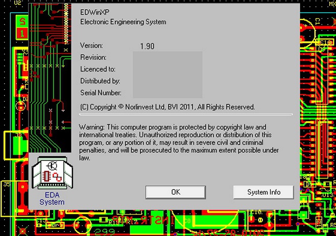
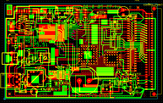
Drawing the PCB, using EdwinXp, results in something like the left picture. every component has its exact outline and
conections predefined in a wast Library, including drilling hole sizes and placements. New and "own" components as
hand made coils and programmambel logics must be defined. From this original drawing with only two layers top =
green and bottom red., a list of drilling holes is created sortedd by size and distance.
This PCB is designed to be used in a rack of several cards with dedicated functions. Interconnected by a sc
backplane, via the connector to the right,
When drawing the possibility to place and solder the component must be considered.


